
TikTok Downloader That Works: Save Videos, Stories, and Audio Free
- January 17, 2026
- Tech
That video you saved to favorites might vanish tomorrow. Creators delete posts, accounts go private, and… Read More
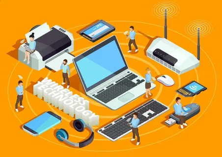
The advances made in wireless technologies of the future have created a high demand for high-frequency PCBs in the field of electronics that is constantly evolving. High-frequency substrates have now become an enabler for enhanced circuit performance because of the integration of 5G networks, rising IoT applications, and enhanced radar, communication apparatus, and facility applications. In high-frequency environments, they ensure speed, stability, and signal quality; and their role is much more than the mere contact point.
High-frequency applications include some special requirements and challenges due to their nature of applications. Any kind of small imperfection in the material or layout can be a problem mainly because the signals move at increasingly higher rates. The use of advanced PCB design has been made necessary because to achieve the best results in the layout and manufacturing of PCBs there is a need to be as accurate as possible, especially in the areas of technological advancement such as the USA. Due to improvements in the electronics manufacturing technology generally relating semiconductor engineering and the pcb design in usa is experiencing the emergence of electronic products having high-speed and high-frequency solutions.
Precision engineering meets material science.
First and foremost, high-frequency PCB design is heavily dependent on the material that is selected for use. The electrical properties of the materials which are used in these applications must be uniform in the range of the operation frequency. Maintaining the dielectric constant ensures a steady signal rate in high-speed systems, eliminating timing inaccuracy and signal (Module: phone synchronization).
High-frequency boards come in a variety of materials and these include hydrocarbon-based laminates, ceramic filled composites or Polytetrafluoroethylene (PTFE). These are associated with lower dielectric losses and the ability to offer the best signal integrity. To accomplish the required mechanical and electrical results, they necessitate certain drilling, plating, and laminating procedures, which add complexity to the manufacturing process.
Simultaneously, the need for boards that can handle quicker signal processing and data throughput is being driven by advancements in semiconductor engineering in the USA. Integrated circuits require PCB substrates that can match their performance levels as they get more powerful. Innovations in both fields have resulted from this mutually reinforcing relationship between PCB evolution and semiconductor development, with each driving the other toward increased efficiency and speed.
Performance and Accuracy in US PCB Design
Because of its significant influence in the consumer electronics, aerospace, defense, and telecommunications industries, the USA continues to lead the world in high-frequency PCB design. Understanding the end-use application thoroughly is usually the first step in the design process. The creation and prototyping of layouts based on simulation come next. The effect of each ground plane, route, and trace on signal behavior is assessed.
In order to forecast how signals would behave in practical situations, high-frequency PCB design in the USA places a strong emphasis on sophisticated design software and modeling tools. By taking into consideration structural mechanics, heat dissipation, and electromagnetic fields, these models guarantee that the finished product operates dependably in all anticipated circumstances.
Additionally, in high-frequency applications, the PCB design board needs to allow for downsizing without sacrificing functionality. The density of components on a single board rises with the size and power of devices. In order to maintain reliable power supply networks and high-speed transmission pathways, designers must come up with innovative solutions to manage space.
The Function of Quality Control and Testing
Testing is a crucial component of the development cycle rather than an afterthought in high-frequency PCB design. Before final deployment, board performance is verified using vector network analysis, time-domain reflectometry, and signal integrity analysis. These techniques identify any variations in power fluctuations, signal reflections, or trace impedance that could jeopardize functioning.
Another essential component of high-frequency PCB evaluation is thermal analysis. Components produce more heat when signals move more quickly. Appropriate heat regulation ensures reliability as well as strength. Due to this heat creation challenge, thermal vias, heat sinks, and complex copper rheostatic arrangements are usually added to the design.
High-frequency PCBs have a greater challenge manufacturing tolerances than traditional boards. Any alterations in copper roughness, dielectric thickness, or trace width will affect the impedance, and thus reduce signal quality. As a result, cooperation between fabrication facilities and designers becomes crucial. Efficient communication and strict adherence to design standards guarantee that the final product is what was intended.
Looking Ahead: Emerging Technologies and High-Frequency Boards
The demand for sophisticated PCB solutions is rising as wireless technologies and high-speed computing continue to progress. High-frequency PCB design is becoming even more important as 6G approaches and applications like augmented reality, and machine-to-machine communication gain traction.
Future developments are being laid by the combination of PCB innovation and semiconductor engineering in the USA. Precision signal routing, power integrity, and thermal control—all characteristics of state-of-the-art PCB engineering—are essential to these sophisticated systems.
By automating intricate layout choices and streamlining high-frequency signal routing, artificial intelligence is also starting to have an impact on PCB design. It is possible to assign thousands of layout scenarios to machine learning algorithms and find the optimal combination of cost, performance, and manufacturing feasibility.
However, due to the increased focus on sustainability in the electronics manufacturing industry, designers are now forced to consider the impacts of the material and methods used in high-frequency boards. To meet regulations as well as the consumer’s demands, the coverings are gradually shifting to lead-free ones, substrates are increasingly recyclable and production is gradually turning energy-efficient.
Conclusion
One of the crucial components in the advancement of new generations of wireless communication technology is high-frequency PCBs. A thorough grasp of materials, signal behavior, and system integration is necessary for both their design and execution. As frequencies increase and form factors decrease, the challenges engineers and manufacturers encounter get more complex, but so do the solutions.
The electronic industry is addressing the performance needs of a hyperconnected society by strategically applying semiconductor engineering in usa and continuously innovating PCB design in the USA. The high-frequency PCB design board is now an active facilitator of speed, accuracy, and technical advancement rather than merely a passive channel for electrical information.
More disciplinary convergence, closer integration of testing and simulation, and a stronger focus on accuracy at all stages of the design and manufacturing process are all part of the future. High-frequency PCBs will assist define what wireless technologies might eventually accomplish in the future, in addition to fostering their development.


Armenia is a land where ancient... Read More

Price movement within limited time spans... Read More

Grooming is an essential part of... Read More
In 2026, there will be a... Read More

Singapore is known for its skyline,... Read More

You know the feeling: you finally... Read More
Clothes have a limited life-span and... Read More

Clothes meet water many times. Home... Read More

Have you ever thought of the... Read More
You found a car that looks... Read More

In the symphony of components that... Read More

That video you saved to favorites... Read More

Posts vanish. Accounts go private. Live... Read More

Introduction: Bright Skin Is Not an... Read More

TL;DR Online MBAs from UGC-approved Indian... Read More

For Indian equity traders and investors,... Read More

If you’ve recently opened a bank... Read More